Silicon atoms can connect to 4 other atoms at a time.
In a pure crystal of silicon, each silicon atom is
attached to 4 others. You can picture a silicon atom
at the center of a cube, connected to two more silicon
atoms at the opposite corners of the top of the cube,
and another two silicon atoms at the opposite corners
of the bottom of the cube.
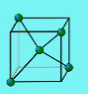
This arrangement keeps the
silicon nuclei as far away from one another as possible.
They arrange themselves this way because they connect
to one another by sharing an electron, so the nucleus
has a slight positive charge, and is repelled away from
the other positively charged silicon nuclei around it.
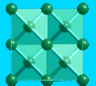
In a pure silicon crystal, the shared electrons are all
locked in place between the silicon nuclei, and are not
free to move around and conduct electricity. A pure
silicon crystal is thus not a very good conductor.
If we add a small amount of some other atom, so that
only one out of a million atoms is not silicon, then
the crystal structure will not change, but the impurity
will be trapped inside the crystal.
If we look at a portion of the periodic table of the elements:
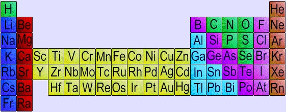
specifically the area around the element silicon:
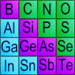
we see that the elements colored in purple
(the natural semiconductors) are adjacent to metals on the
left (like Aluminum, Galium, and Indium),
and non-metals on the right (like Phosphorus).
Elements to the left of silicon, like Boron or Aluminum,
connect to only three other atoms at a time. Elements to
the right of silicon, such as Phosphorus, connect to five
other atoms at a time.
If we replace every millionth atom of silicon in our
crystal with an atom of phosphorus, it can only connect
to four silicon atoms, since the crystal structure
only has four silicon atoms near the phosphorus atom.
The phosphorus has an electron left over that is not
strongly attached to any nucleus, and it can be knocked
free fairly easily.
Because a silicon crystal with extra phosphorus has free
electrons (which carry a negative charge) it is called
"N" type silicon, where the N means "negative".
If we replace every millionth atom with Boron or Aluminum,
which can only attach to three other atoms, we have a
crystal that has a missing bond in it, between the boron
atom and a silicon atom. An electron from the boron atom
fills in this bond, leaving the boron nucleus with a
positive charge. We call such a crystal "P" type silicon,
for "positive".
The interesting things start to happen when we place
N type silicon next to P type silicon.
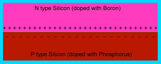
The positively charged boron nuclei attract the free
electrons of the phosphorus atoms. The electrons cross
over from the N type to the P type. This leaves the
N type silicon slightly positive, and makes the P type
silicon slightly negative.
As more electrons migrate to the P type, the P type
gets more negative. Because it is negative, it repels
electrons, making it harder for more electrons to migrate.
When so many electrons have migrated that the P side is
0.7 volts more negative than the N side, no more electrons
can migrate, and the process stops.
The phosphorus atoms near the junction between the two
types are depleted of their free electrons. Those electrons
have filled in the missing bonds between the boron and
silicon atoms on the other side, so no electrons can move
into those spaces. Since there are no free charges to move
around in the space near the junction, we say it is
depleted of charge carriers, and it is an insulator.
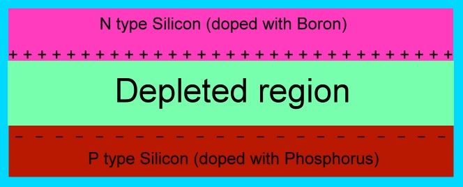
On one side of the depleted region is positively charged
N type silicon, and on the other is negatively charged P
type silicon. If there were any electrons free in this zone,
they would be attracted to the positively charged N type
silicon.
If a photon of light hits one of the atoms in this region
with enough energy, it can knock an electron loose from
the atom. This electron will move towards the positively
charged N type silicon. Electrons on the other side of
the atom will move in to fill the hole, moving towards the
positive side of the junction.
The photon of light has thus created a situation where an
electron has moved away from the depleted area and into the
N type silicon, leaving the P type silicon with a positive
charge. It can't move back, because the depleted region
has 0.7 volts pushing it away.
If we connect a wire to each of the two types of silicon,
and attach those wires to a light bulb, the electron will
push on the electrons in the wire, moving them through the
light bulb. At the other end, an electron from the wire
will move into the P type silicon, replacing the electron
that was knocked free by the photon.
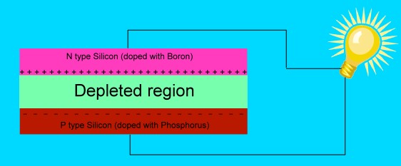
If enough photons are hitting the junction area, electrons
moving through the light bulb will cause the filament
to heat up, and the light bulb will glow.